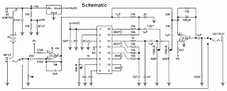
PT2399 Echo, Reverb Effects Schematic Circuit
IC PT2399 from Princeton Technology Corporation. Pin 15 and pin 16 to form a capacitance by changing the external resistance to change the input frequency response of the inverting amplifier, as the signal input. Pin 8, pin 9, pin 10 form an external pre-emphasis - Compare the source set, the internal microcontroller output DO0 after passing through the circuit compared with the input signal, thus completing the A / D conversion, and then 1bit of data into the microcontroller the Delay Line.
Similarly, pin 11, pin 12 and pin 7 form to add - Compare source circuit, the signal from pin 12 out. And pin 13 , pin 14 is a separate inverting amplifier, and not directly connected with the internal processing circuitry, it can be used flexibly for the designers.
Pin 6 to control the speed of the internal MCU Delay Line VCO input, changing the voltage can change the delay time, and from pin 5 to monitor the current oscillation frequency. Pin 2 for the internal op amp reference when a single supply source, the integrated circuit is well within 1/2 partial supply voltage, so only the external access to anti-ripple circuit (voltage regulator) to.
PT2399 frequency response within the limits of about 5kHz, and when the input signal when the frequency is higher than 4kHz, sine wave input signal will become somewhat similar to the triangle wave, and in the input signal frequency is greater than 5kHz, it will produce distortion and digital noise.
Although the guitar signal in the above information on this range is relatively small, but the delay of the chip to deal with these frequency response will be smooth and some distortion.
PT2399 input signal amplitude is about 3Vpp signal level higher than this range will be limiting. In the above diagram, the change of pin 15, pin 16 of the resistive and capacitive components, you can change the input frequency response; change components on pin 12 , pin 13, pin 14 of the resistive and capacitive components, you can change the output frequency response.
The internal structure of integrated circuits based on PT2399, the two parts of the design is the operational amplifier filter design, designers can calculate the actual situation, to not repeat them here.
In addition, PT2399 VCO external setting resistors to the minimum, the delay time is 31.3ms, because of this a long time, not suitable for production of chorus or Flanger effects.


Hiç yorum yok:
Yorum Gönder